> Energy band gap>
GaAs |
AlxGa1-xAs |
InxGa1-xAs
> Refractive index
> GaAs |
AlAs |
AlxGa1-xAs |
InxGa1-xAs
> Devices
> Bragg mirror |
RSAM |
SA |
SANOS |
SOC |
Microchip |
PCA
> Device application
> Papers |
Patents |
FAQs
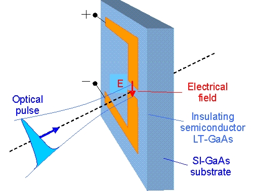
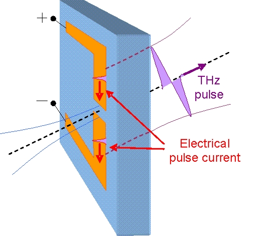
PCA - Photoconductive Antenna
PCA construction and application
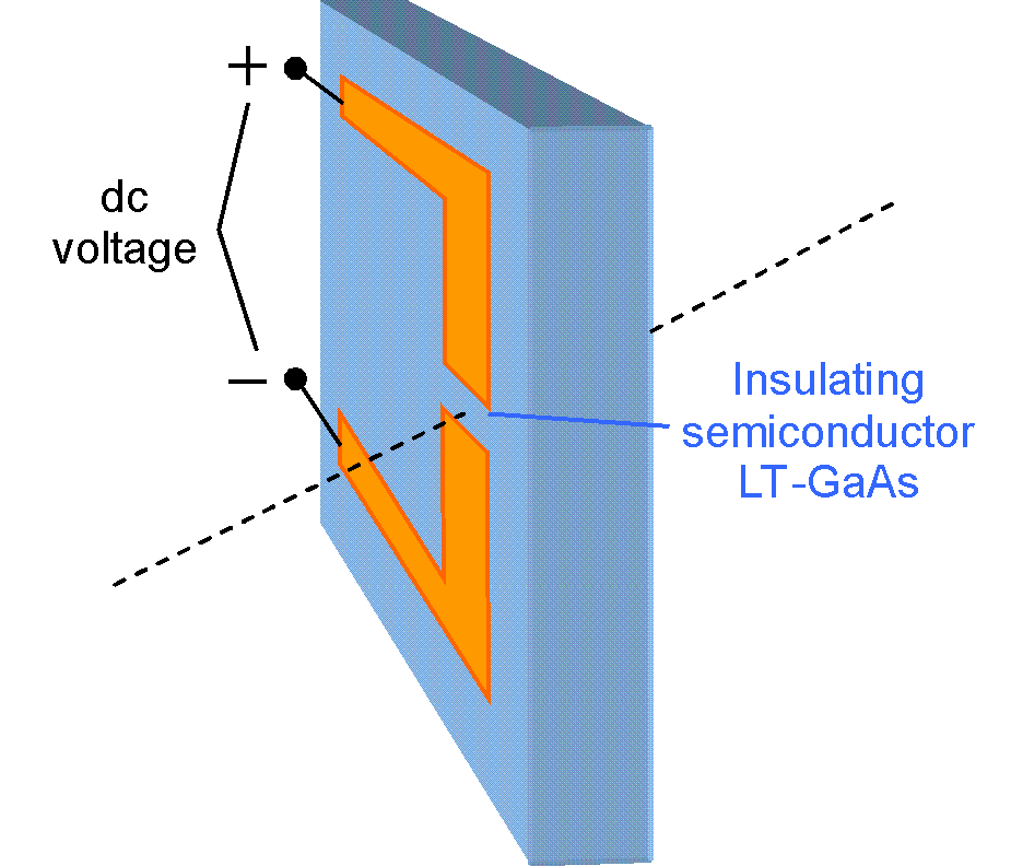
Construction:
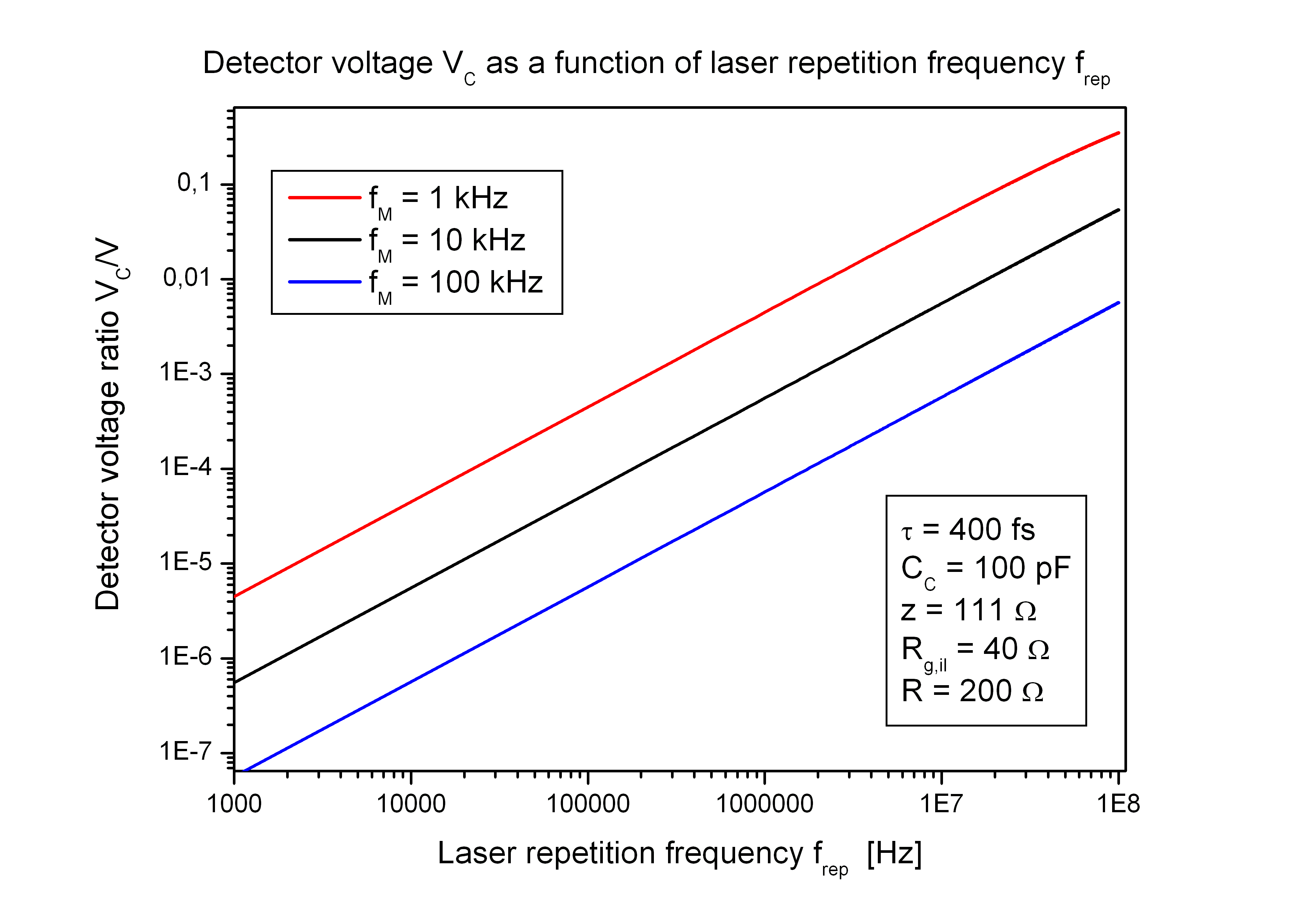
- A photoconductive antenna (PCA) for terahertz (THz) waves consists of a highly resistive direct semiconductor thin film with two electric contact pads. In most cases the film consists of a III-V compound semiconductor like GaAs. It is epitaxially grown on a highly resistive semi-insulating GaAs substrate (SI-GaAs).
- The important difference between the SI-GaAs substrate and the film is the relaxation time for excited carriers. In a SI-substrate the carrier lifetime is about 20 ps, but in the film shorter than 1 ps.
Behaviour:
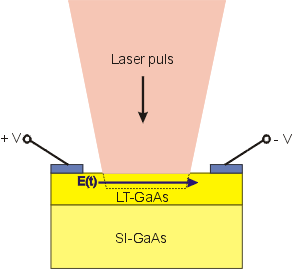
- A short laser puls with puls width < 1 ps is focused between the electric contacts of the PCA. The photons of the laser pulse have a photon energy E = hν larger than the semiconductor energy gap Eg and are absorbed in the film.
- Each absorbed photon creates a free electron in the conduction band and a hole in the valence band of the film and makes them for a short time electrical conducting until the carriers are recombined.
- To get the needed short carrier lifetime the film must include crystal defects. These defects can be created by ion implantation after the film growth or alternatively by a low temperature growth. Low temperature grown GaAs (LT-GaAs) between 200 and 300 °C contains excess arsenic clusters. These clusters create defect levels within the band gap Eg and lead to a fast non-radiative recombination of the electron-hole pairs within a time interval < 1 ps.
Application:
- The PCA can be used as THz transmitter as well as THz receiver
- In case of a transmitter a voltage V is connected on the electrical contacts and the excited carriers are accelerated by the electric field during the optical pulse resulting in a short broadband electromagnetic pulse with a time-dependent electrical field E(t) and frequencies in the THz region.
- In case of a THz receiver an amplifier is connected on the electrical contacts. During the optical pulse the excited carriers are accelerated by the electric field component of the incident terahertz pulse with the time-dependent electrical field E(t). This leads to a voltage signal across the antenna gap.
• PCA application
PCA application
The PCA can be used as a THz emitter or detector in
pulse laser gated broadband THz measurement systems for time-domain spectroscopy.
Because THz waves penetrate dielectric materials like paper or plastic, are reflected by
materials with free electrons like metals and are absorbed by moleculs with
certain vibration levels within the terahertz band they have a lot of applications in the
fields of time-domain spectroscopy and imaging.
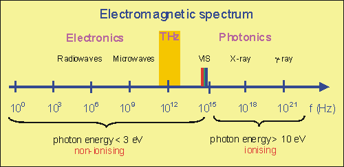
Note: Terahertz radiation is nonionizing. That means it is safe.
Process control
- Polymeric compounding.
- Examining circuit interconnects in packaged ICs.
- Final control of packaged products.
- Quality control in food processing.
- Rapid characterisation of the stability and polymorphic forms of drugs.
Security checks
- Screening passengers for explosives and weapons
- Luggage screening
- Mail drug screening
- Reading text in envelopes or beneath paint.
• Frequency and wavelength
Frequency and wavelength
The photoconductive antenna can be considered as a dipole of length L which is in resonance with
the electromagnetic wavelength λn inside the semiconductor.
The resonance condition is L = m · λn/2 with m = 1, 2, 3,.. integer.
The wavelength λn in the material with refractive index n can be approximated by λn = λ/n.
Using the wave relation c = λ · f and m = 1 the resonance frequency f of the antenna can be estimated as f = c/(2 · n ·L) with
- c = 3 · 108 m/s - speed of light in vacuum.
- n - refractive index of the semiconductor antenna material.
- L - length of the antenna dipole.
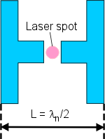
The refractive index n of GaAs at terahertz frequencies is n = 3.4. With this value the first resonant frequency and wavelength of the antenna with length L can be calculated as follows:
| f (THz) | λ (µm) | L (µm) |
|---|---|---|
| 0.3 | 1000 | 147 |
| 0.5 | 600 | 88 |
| 1.0 | 300 | 44 |
| 1.5 | 200 | 29.4 |
| 3.0 | 100 | 14.7 |
• Focusing the optical beam on the antenna gap
Focusing the optical beam on the antenna gap
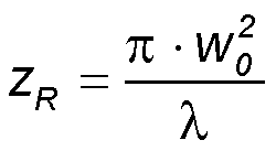
The semiconducting gap in the center of the antenna must be illuminated by a focused laser beam. If we consider a Gaussian beam then the beam width w(z) along the beam axis z and the Raygleigh range zR are
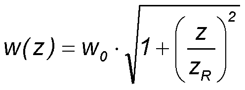 and
and
The diameter of the beam width 2·w0 at the focus point z = 0 is
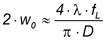
with λ - laser wavelength, fL - focal length of the lens, D - diameter of the laser beam at the focusing lens.
To ensure that the focused beam diamter 2·w0 is somewhat larger then the antenna gap distance g the focal length fL of the focusing lens must be
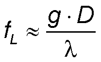
In case of g = 5 µm, D = 1 mm, and λ = 800 nm the focal length of the lens must be fL ~ 6 mm.
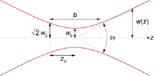
Gaussian beam width w(z) as a function of the distance z along the beam axis. w0 - beam waist; b - depth of focus; zR - Rayleigh range; θ - asymptotic beam divergence.
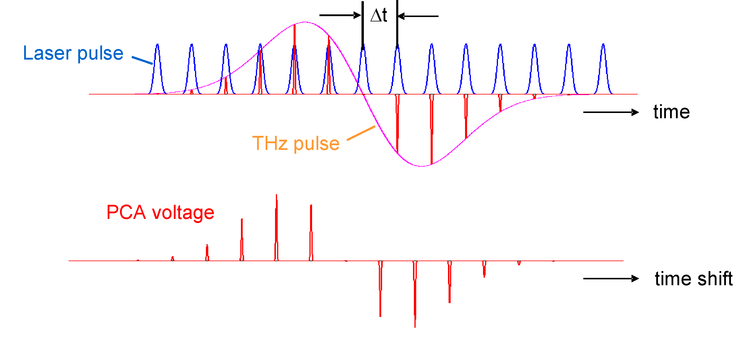
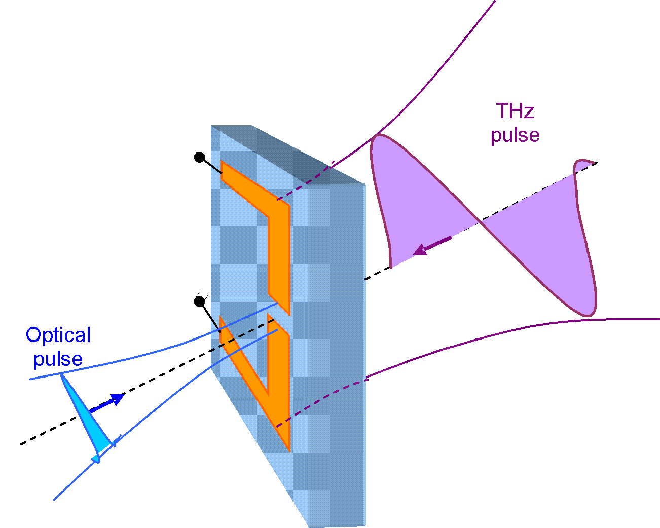
• THz pulse emission
THz pulse emission
Phase 1: Antenna before illumination
- The semiconducting antenna gap is highly resistive. No free electrons are in the conduction band.
- A supply voltage V between the two antenna contacts results in an electric field
in the semiconducting antenna gap between the metal contacts. The electric field strength is E = V/g
(g - gap distance).
With a typical supply voltage of 10 V and a gap distance of 5 µm the electric field strength is E = 2·106 V/m. - The optical pulse must be focused onto the semiconducting antenna gap in such a way, that the spot diameter 2·w0 is slightly larger then the gap distance g so that the metal lines are also illuminated.
Phase 2: Optical pulse meets the antenna gap
- A short optical pulse meets the antenna gap. The optical energy is absorbed and free carriers are created in the semiconductor material. Each absorbed photon creates a free electron.
- The free electrons follow the electric field creating a short current pulse j(t) in the semiconducting gap material.
- Typical values for the optical pulse are: Pulse duration τ ~ 100 fs, Pulse energy E ~ 100 pJ, Pulse repetition rate frep ~ 100 MHz, Average optical power Pav ~ 10 mW.

Phase 3: THz pulse emission
- An electromagnetic field is emitted by the dipole as long as the current pulse changes with time.
- At first the current increases during the illumination of the gap and emits the first part of the THz pulse.
- If the current decreases because the electric field is subsequently compensated by the transferred carriers then the second part of the THz pulse is emitted with a reverse polarization direction.
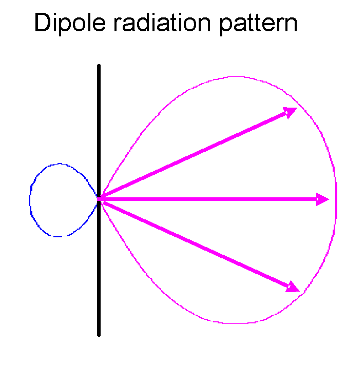
- The THz pulse is emitted around the dipole with a polarization direction of the electric field parallel to the dipole axis.
- Most of the electromagnetic energy is emitted into the half space of the semiconducting substrate material with high refractive index n ~ 3.4 (magenta in the figure right). Therefore the emitted THz pulse in the substrate direction shall be collected for measurements.
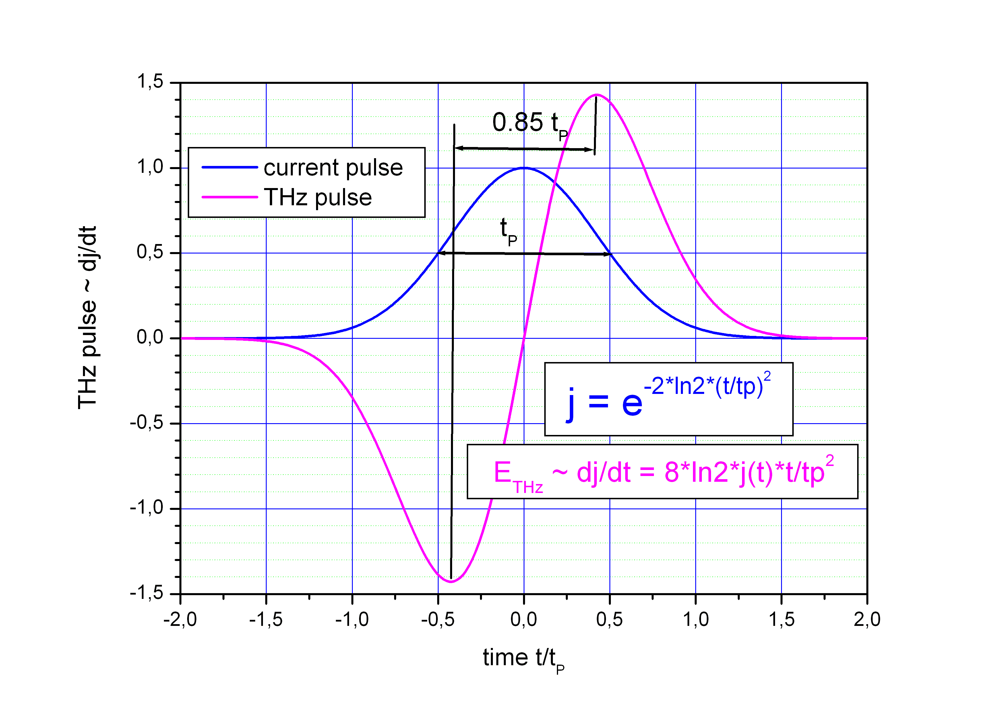
THz pulse shape
- The time dependence of the current j(t) in the dipole can be assumed as Gaussian pulse with pulse duration tP.
- The emitted electric THz field ETHz is proportional to the time derivative of the current: ETHz ~ dj/dt.
- The THz pulse duration is therefore proportional to the current pulse duration with a value ~ 0.85·tP.
- The current pulse in the semiconductor antenna gap initiates a current pulse in the antenna metal contacts.
- The pulse velocity vP in the dipole contacts is vP ~ c/n (n ~ 3.4 refractive index of the GaAs semiconductor substrate).
- The current pulse duration tP,dipole in the dipole metal contacts depends on the dipole length L: tP,dipole ~ L/(2vP)~L·n/(2c).
- Example: L = 100 μm ⇒ tP,dipole ~ 10-4m·3.4/(2·3·108m/s) ~ 0.57 ps.
⇒ The THz pulse has the shape of the derivative of a Gaussion pulse. It is longer then the optical pulse because it is determined by the antenna length L.
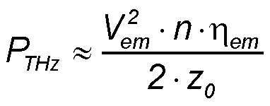
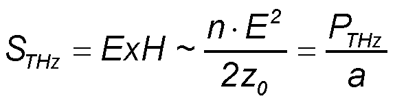
Emitted THz power
The time averaged Poynting vector ⟨S⟩ of the emitted electromagnetic field inside the material with refractive index n (GaAs substrate, silicon substrate lens) can be estimated as
The strength of the emitted electric THz-field ETHz can be roughly estimated by the electric field on
the emitting dipole with length L and supply voltage Vem including a factor ηem which describes
the conversion efficiency between the static electric field Vem/L on the antenna dipole and the emitted THz-field.
ηem depends on the free carrier production in the semiconduror gap by the laser pulse.
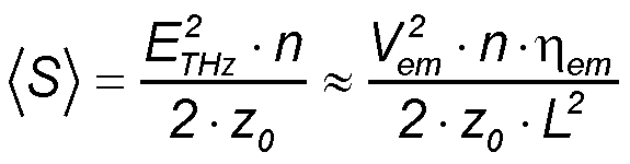
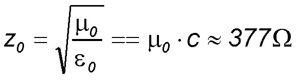
z0 is the characteristic impedance in free space
The emitted THz pulse power PTHz can be estimated using the dipole emitting area L2
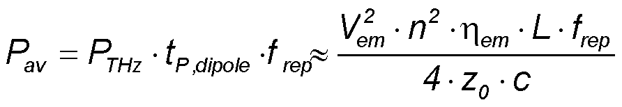
Then the mean THz power Pav averaged over the time inteval between two laser pulses 1/frep is
Example:
With the parameters Vem = 10 V, n = 3.4, ηem = 0.2, L = 100 μm,
frep = 100 MHz we can estimate the pulse power PTHz ∼ 90 mW and the average emitted THz
power Pav ∼ 5.1 μW.
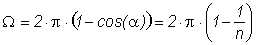
• Escape angle of the THz radiation, PCA without substrate lens
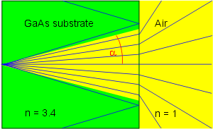
Escape angle of the THz radiation
Because of the high refractive index n ~ 3.4 of the semiconductor PCA the outgoing terahertz waves are strongly diffracted at the substrate-air interface. The boundary angle α for the total reflection can be calculated as
α = arcsin(n-1) ~ 17.1 °
Only THz waves emitted in the solid angle Ω with
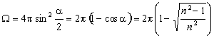
can escape the substrate. For GaAs with n = 3.4 the escape solid angle is Ω = 0.088 π sr = 0.28 sr. This is only 4.4 % of the forward directed intensity.
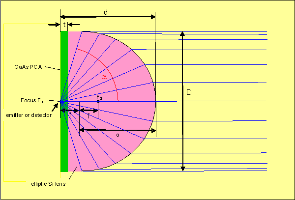
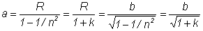
• Aplanatic hyperhemispherical lens
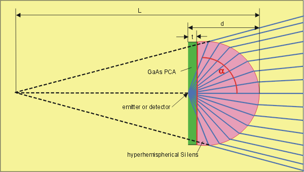
Hyperhemispherical silicon lens
To increase the escape cone angle α a hemispherical lens with the same refractive index n as the PCA can be used. To decrease the divergence in air a hyperhemispherical lens with a certain distance d between emitter and lens tip is common. If this distance d is

then the hyperhemispherical lens is aplanatic, that means without spherical and coma aberration.
For a silicon lens with almost the same refractive index n ~ 3.4 as GaAs at
terahertz frequencies the distance is d = 1.29 R with lens radius R. The height h
of the aplanatic hyperhemispherical lens is therefore h = d - t with the thickness t of
the semiconductor PCA.
The length L from lens tip to the virtual focus behind the lens is given by
L = R (n+1)
For silicon is L = 4.4 R. With this hyperhemispherical lens nearly all the forward directed
terahertz intensity can escape the PCA. The collection angle is α = 73.6 ° and the solid angle for the collected THz beam
is Ω= 1.43 π sr = 4.51 sr.
The problem left is the beam divergence, which requires a further focusing element like a lens or mirror.
• Collimating elliptic lens
Collimating elliptic lens
With an elliptical lens (truncated ellipsoid) with refractive index n equal to that of the PCA a collimated THz beam can be realized if the following relations are fulfilled:
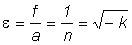
Eccentricity
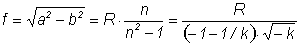
Focal length
Conic constant
Distance d (lens thickness)
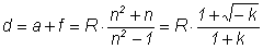
Here R is the radius of curvature at the intersection of the ellipsoid with the optical axis. The lens parameters scales with R.
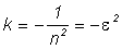
The conic constant k = -1/n2 is related to the standard equation for an aspheric lens:
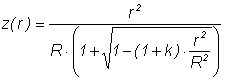
where the optic axis is presumed to lie in the z direction, and z(r) is the sag—the z-component of the displacement of the surface from the vertex, at distance r from the axis.
The antenna is located at the focal point F1 on the major axis of the truncated ellipsoid. The ellipse is characterized by the following parameters:
semi-major axis
Semi-minor axis
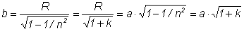
The collection angle is
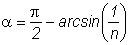
The solid collection angle is
The lens diameter is
For an elliptic collimating silicon lens with n ~ 3.4 the conic constant is k = -0.086, the eccentricity ε = 0.294, the lens diameter D = 2.09 R, the collection angle α = 72.8° and the solid collection angle Ω = 1.41π sr = 4.44 sr.
• THz pulse detection
THz pulse detection
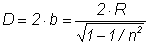
THz pulse measurement in a Time-Domain Spectrometer (TDS)
- The time dependency of the incoming THz electric field is measured by sampling it by a very short optical pulse.
- A photoconductive antenna (PCA) is used as fast electrical switch.
- The antenna gap is conducting only during its illumination by an optical pulse.
- The time shift between THz and optical pulse is changed stepwise with a time increment Δt.
Sampling of THz pulse 1
- Antenna before the THz pulse and the optical pulse arrive ⇒ no voltage on the dipole antenna.
- The THz pulse approaches from back side through the GaAs substrate.
- The THz pulse is focused onto the antenna dipole.
- A short optical gate pulse approaches from front side.
- The optical pulse is focused on the semiconducting antenna gap.
Sampling of THz pulse 2
- The THz pulse meets the antenna.
- The electric THz field induces a voltage between the two antenna halfs.
- The laser pulse creates free electrons in the antenna gap ⇒ a current flows through the gap.
- An electrical charge is shifted from one antenna half to the other.
- The amount of the transferred charge and the resulting antenna voltage are proportional to the applied THz field strength.
Sampling of THz pulse 3
- The optical pulse has passed the antenna.
- No free carriers in the antenna gap ⇒ the gap is insulating.
- The before shifted electrons are stored in one antenna halfe.
- A static voltage can be measured between the antenna halfs.
- The PCA is used as ″ sample and hold ″ device.
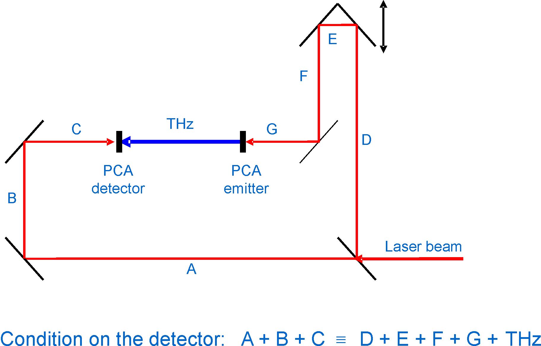
Set-up of a THz time-domain spectrometer
- The time management in a time-domain spectrometer (TDS) determines the set-up.
- The beam of a short pulse laser is divided into the emitter path D+E+F+G and the detector path A + B + C.
- The emitter converts the incoming optical pulse into an outgoing THz pulse.
- At the detector the otical pulse samples the electric field strength of the incoming THz pulse.
- The time delay between the THz and optical pulse on the detetcor can be adjusted by a mechanical delay stage which changes the beam paths lengths D and F.
Detector voltage 1 - THz field strength
- In the example above the emitted THz peak power is PTHz ∼ 90 mW.
- The reflection loss on the silicon substrate lenses at the emitter and detector adds to about 50 %, so that PTHz ∼ 45 mW arrive at the detector area a.
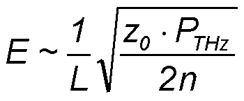
- The THz energy flux on the detector can be described by the Pointing vector STHz.
- If we estimate the diffraction limited THz spot area a ∼ (2·L2) then the peak electric field strength E on the detector dipole with length L and the peak voltage V can be calculated to V = E·L
Example:
With the values PTHz ∼ 45 mW, z0 ∼ 377 Ω, n = 3.4 the peak voltage
V on the detector dipole can be estimated to 1.6 V.

Detector voltage 2 - Equivalent circuit
- The antenna gap resistance Rg depends on the illumination.
- The antenna current is limited by the wave impedance z in space with refractive index n and the illuminated gap resistance Rg,il.
- The resistance R of the antenna contact lines connects the antenna dipole with the electric cable .
- The coaxial cable builds an integrator with large capacitance CC
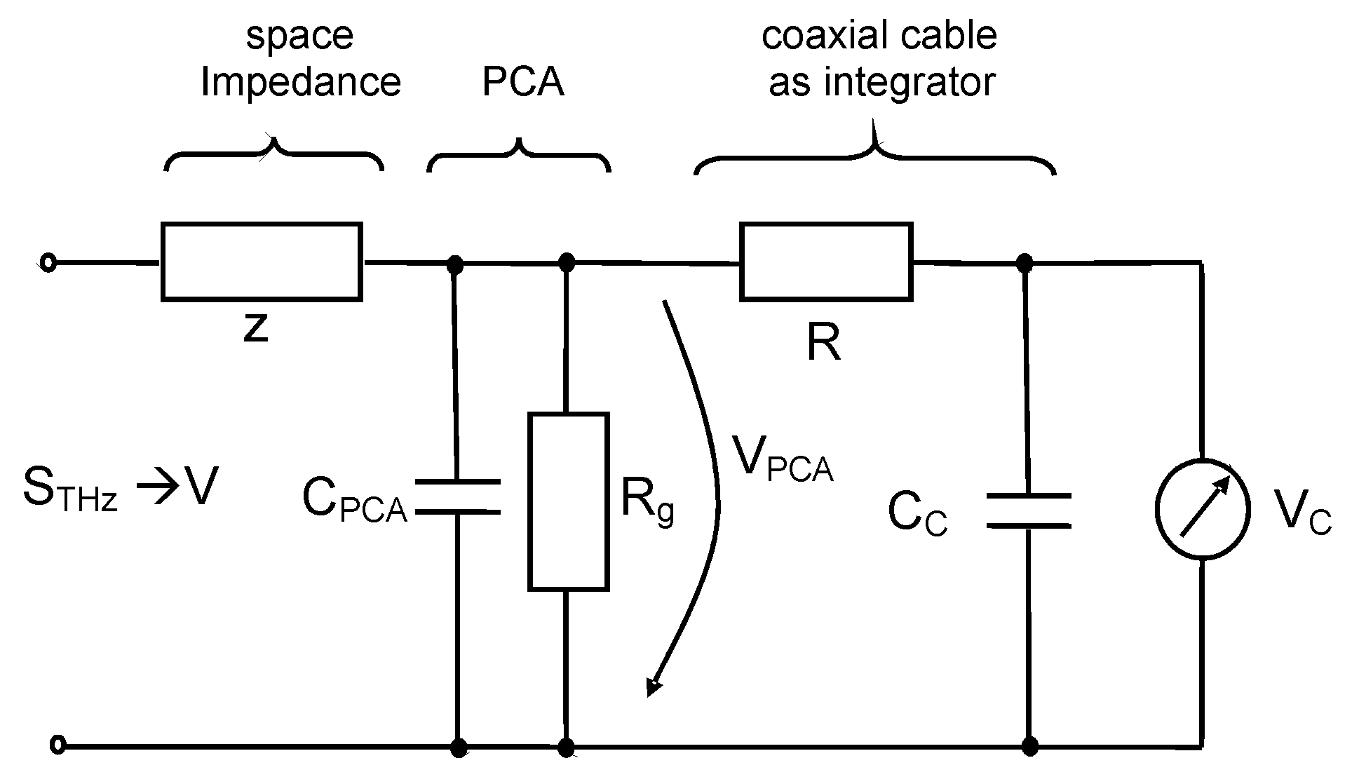
Equivalent circuit for detector antenna with cable
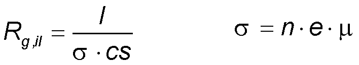
Detector voltage 3 - Illuminated gap resistance Rg,il
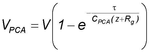
- The voltage VPCA on the antenna capacity CPCA depends on the current in the gap and the free carrier relaxation time τ.
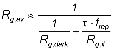
- The non-illuminated gap resistance Rg,dark is very large (insulating gap). In this case is Rg,dark · CPCA >> τ and the stored antenna voltage VPCA ∼ 0.
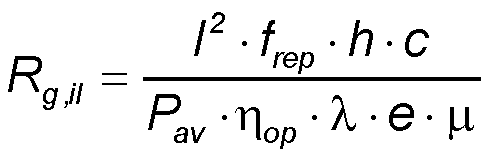
- The illuminated gap resistance Rg,il depends on the gap length l, electrical conductivity σ, and gap cross section cs
- The electrical conductivity σ is proportional to the density of free electrons n and the electron mobility μ (e - electron charge) per gap volume l·cs.
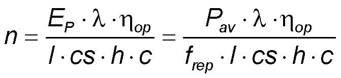
- The electron density n can be calculated assuming it is given by the ratio of optical pulse energy EP and photon energy h·c/λ. A conversion efficiency ηop describes that some of the incoming photons are reflected or transmitted at the gap and do not create free electrons.
- The optical pulse energy EP can be calculated with the average optical power Pav on the antenna gap and the repetition frequency frep of the pulse laser.
- The average illuminated gap resistance R g,av which can be easily measured by a resistance tester, can be estimated with the relaxation time τ of the excited electrons and the pulse repetition rate frep.
Example:
With the values l = 5 μm, frep = 100 MHz, Pav 10 mW, ηop ∼ 0.2,
λ = 780 nm, μ ∼ 0.05 m2/(V·s), Rg,dark ∼ 10 MΩ, τ ∼ 400 fs
we can estimate R g,il ∼ 40 Ω and R g,av ∼ 900 kΩ.
Detector voltage 4 - Cable output voltage VC
- During the optical pulse a certain amount of electrons is transferred over the gap resulting in the voltage VPCA ∼ V on the antenna dipole capacity CPCA as long as the illuminated gap resistance is Rg,il < z.
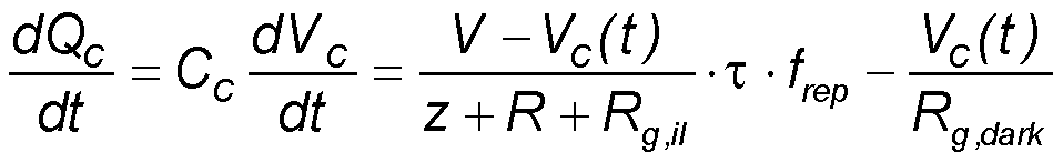
- In the time interval T = 1/frep between optical pulses these electrons pass the resistance of the antenna contact lines R and distribute in the connected cable with capacity CC resulting in a reduced voltage VC = VPCA · CPCA / CC.
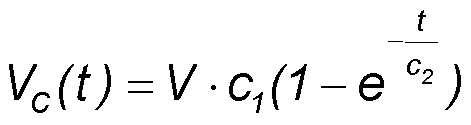
- As long as the time shift between the incoming THz pulse and optical pulse on the antenna is unchanged the charge in the cable and the corresponding average voltage VC(t) increases with each pulse until the cable voltage approximates the antenna voltage VC ∼ VPCA ∼ V.
- If a modulation of the emitter antenna voltage is used then the integration time is limited up to the change of the emitter antenna polarity. This results in VC << V.
Rate equation for cable charge QC:
Example:
With the values τ = 400 fs, frep = 100 MHz, Rg,dark = 10 MΩ, z =z0/nSi = 377 Ω/3.4 = 111 Ω,
Rg,il = 40 Ω, R = 200 Ω, CC = 100 pF we get c1 = 0.53 and c2 = 0.47 ms.
- If a modulation frequency fmod of 10 kHz for lock-in detection is used then the detector signal is integrated
over a time interval tM = 1/(2·fmod) = 0.05 ms.
It can be seen in the graph right that in this case the detector signal decreases if the dark resistance Rg,dark of the PCA decreases below ∼ 1 MΩ.
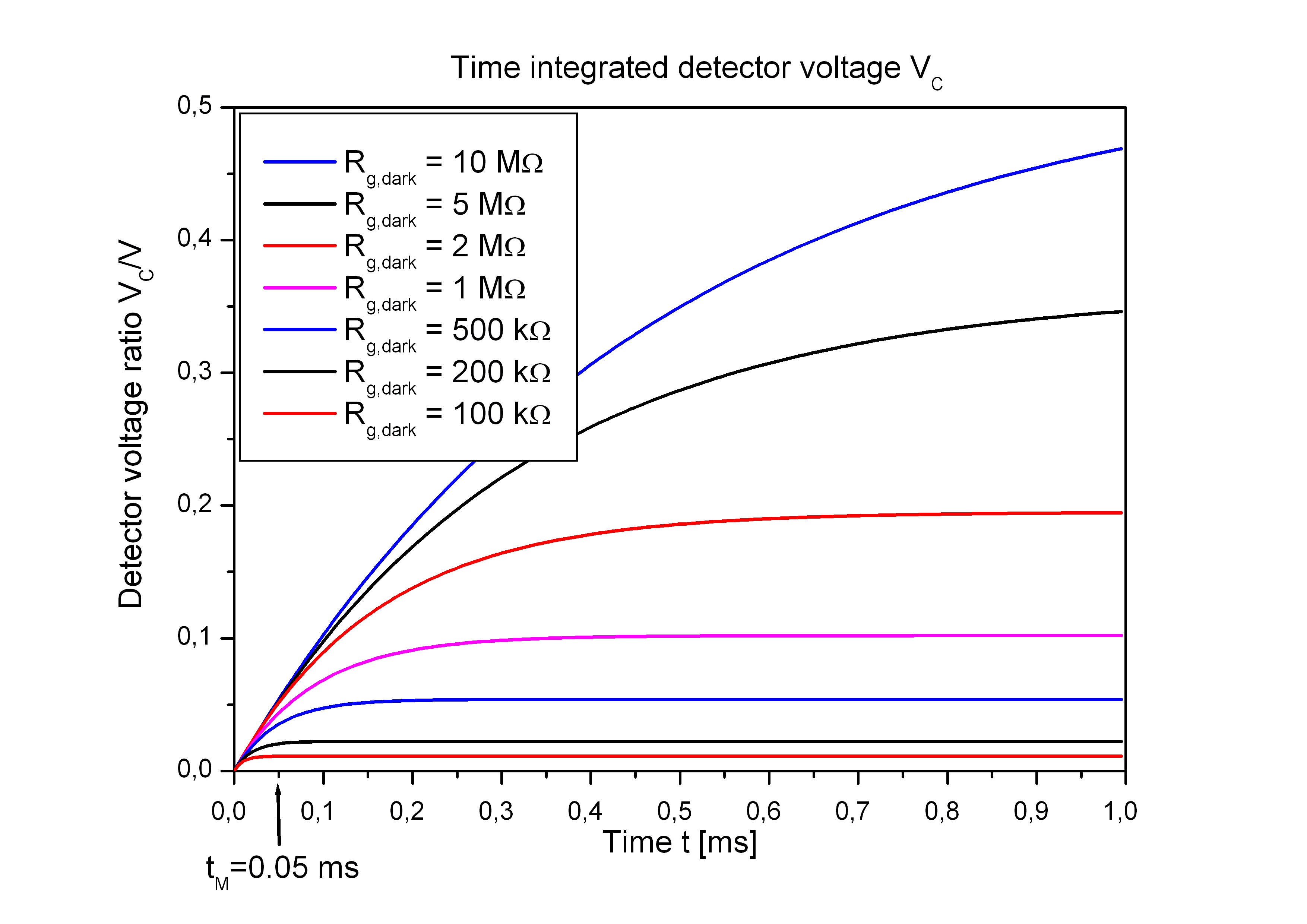
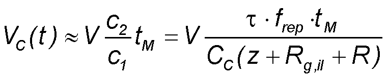
Detector voltage 5 - Dependence on repetition frequency frep
- If the half period tM = 1/(2·fM) of the modulation frequency fM is tM << c2 then the detector voltage VC on the cable is proportional to tM and frep.
- During the time tM the detector output voltage VC increases linear with each incoming terahertz pulse.
- To collect on the detector output a large signal voltage a high laser repetition rate frep ∼ 100 MHz is needed.
- Therefore a laser source with a low repetition rate in the kHz region is not appropriate to drive a THz time-domain spectrometer with photoconductive antennas.
Approximation for t = tM << c2